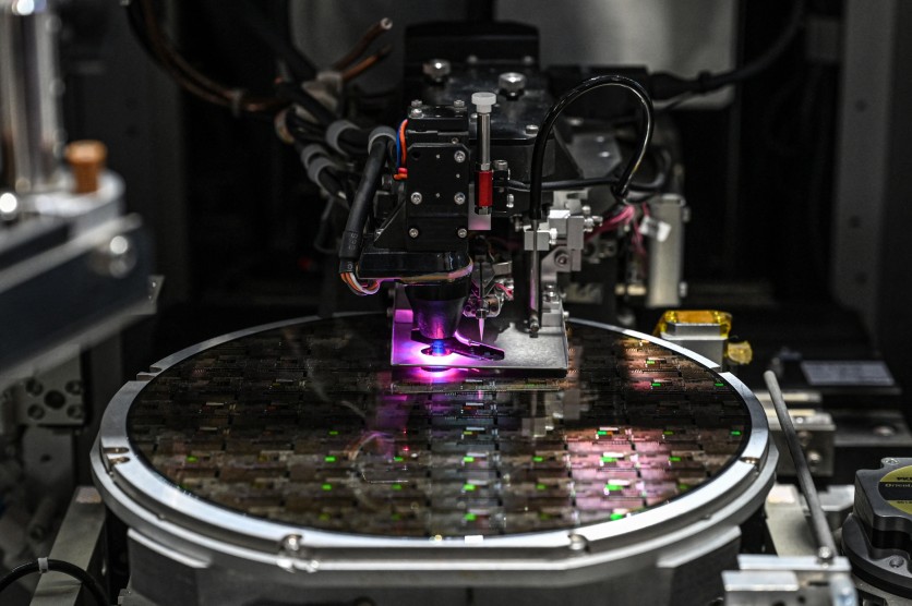

Jade GAO/AFP via Getty Images
China’s top economic planning body declared this morning that the country’s semiconductor supply chain had become “significantly safer” — the most confident official assessment Beijing has issued on chip self-sufficiency since the US-led export control campaign began in earnest in 2022. Li Chao, spokeswoman for the National Development and Reform Commission (NDRC), described a transition to full-chain synergy at a press briefing, moving from “isolated technological breakthroughs” to “full-chain industrial synergy.” That claim is grounded in a real and verifiable milestone: by 2025, China’s domestic chip equipment share reached 35% of all semiconductor manufacturing equipment installed in Chinese fabs, up from 25% the year before and well above the 30% target Beijing had set for itself.
The number is real. What the NDRC did not headline is what it takes to reach 70% — the target Beijing has set for 2027 — and where the remaining gap actually sits. The distance between today’s 35% and tomorrow’s 70% is not evenly distributed across the chip toolchain. In the most visible process steps, domestic tools have already captured dominant share. In the layers beneath those tools — the radio-frequency power supplies, precision vacuum valves, and high-purity quartz parts that go inside the equipment — China remains 80% to 90% dependent on foreign suppliers. These are the components US export controls already cover. They are what the industry calls the hidden chokepoint in China’s supply chain, and they are the reason “full-chain industrial synergy” is a description of a direction, not a destination.
Where China Actually Won: Etching, Deposition, and NAURA at SMIC
The progress at the tool level is specific and documented. Three Chinese equipment makers — NAURA Technology Group, AMEC (Advanced Micro-Fabrication Equipment Inc. China), and ACM Research Shanghai — ranked among the world’s top 20 semiconductor equipment suppliers by sales volume for the first time in 2025. Their combined domestic market share at Chinese fabs reached 45% to 50% for the categories they compete in.
In the category where localization has gone furthest, the numbers are striking. NAURA’s oxidation and diffusion furnaces now account for 60% of SMIC equipment deployed on SMIC’s 28-nanometer (nm) production lines. Thermal processing overall has reached 30% to 40% domestic penetration across Chinese fabs. Etching and thin-film deposition — the two categories where AMEC and NAURA compete most directly with Lam Research and Applied Materials — have crossed the 40% domestic mark. AMEC’s 5-nm etching tool entered validation on TSMC’s advanced-process lines, a signal that at least one Chinese tool has cleared the most demanding qualification in the industry. Piotech, a deposition specialist, doubled its installed share of plasma-enhanced chemical vapor deposition equipment at YMTC’s 3D NAND production lines in 2025, lifting its position from 15% to 30%.
NAURA orders booked through Q1 2027, according to China Semiconductor Industry Association data cited by multiple industry outlets. NAURA’s revenue is on pace to reach somewhere between 46.8 billion and 52.0 billion yuan (approximately $7.0 billion to $7.7 billion) in 2026, representing roughly 30 times its revenue level a decade ago.
This progress is not accidental. Beijing now requires 50% domestic equipment for fabs as a condition of fab-expansion approval — a mandate that has turned domestic tool qualification from a voluntary preference into an operational prerequisite. Big Fund III, the third phase of China’s state-directed semiconductor investment vehicle, was established in 2024 with registered capital of 344 billion yuan, the Ministry of Finance holding the largest stake at 17% and China Development Bank Capital and major state-owned banks among the other 18 investors. Big Fund III differs from its predecessors in where its priority sits: unlike the earlier phases, which focused on chip design and manufacturing, the current round places its emphasis squarely on chipmaking materials and manufacturing equipment — the layers the NDRC now cites as evidence of a safer supply chain. DigiChina’s analysis of China’s 15th FYP confirms equipment and materials as core investment priorities in the current round.
The Hidden Chokepoint: What Goes Inside the Tools
Equipment localization statistics measure tools. They do not measure the components that make those tools run.
A plasma etching chamber — the type that AMEC and NAURA manufacture for etch steps in chip production — requires a radio-frequency (RF) power supply to excite process gas into a plasma state. That plasma, a charged mixture of ions and reactive radicals, strikes the wafer surface and selectively removes material with the geometric precision that carves circuit features at the nanometer scale. Without the RF power supply delivering precisely controlled waveforms at 13.56 megahertz (and at secondary frequencies of 400 kilohertz, 2 MHz, or 60 MHz for independent ion-energy control), the etching chamber does not function. The global RF power supply market is dominated by MKS Instruments, Advanced Energy Industries, and Comdel — all American companies — which collectively hold 65% to 75% globally. China’s domestic RF power supply penetration stands at approximately 20% — and primarily for mature-process tool configurations. High-power RF supplies for advanced-process etch, which require 10 kilowatts or more of precisely delivered power, remain in what the industry calls “localization-attack mode”: actively being developed, but not yet in widespread production deployment.
The precision vacuum valve situation is more acute. The tool categories where China has made its most visible localization gains — etch chambers, chemical vapor deposition (CVD) reactors, diffusion furnaces — all depend on precision valves to control the gas flows that define the process environment inside the chamber. VAT Group holds precision valve market, a Swiss manufacturer, commands approximately 60% to 70% of the global precision vacuum valve market. China’s domestic valve manufacturers, including Zhejiang Gutai and Shanghai Zhongxi, are at an early stage of capability for mature-process configurations. High-end chamber valve penetration under 10% — the lowest of any major sub-component category. Quartz parts — the high-purity tubes and chamber liners used in thermal processing, etch, and CVD — sit in the 30% to 40% domestic range, ahead of valves but still heavily reliant on Japanese and US suppliers.
This is the arithmetic behind the gap between 35% and 70%. The tool-level localization rate measures what is visible. The sub-component layer measures what sits underneath. At the tool level, China cleared 35% in 2025 and is targeting 70% by 2027. At the sub-component level, the leading constraint — precision valves — sits under 10%.
There is a further implication that the NDRC’s “significantly safer” framing does not address. The upstream sub-components the industry calls the “hidden chokepoint” are not merely a risk the US could choose to target. They are already covered by the US Export Administration Regulations (EAR). The export control perimeter does not stop at finished tools. It extends to the EAR covers upstream sub-components inside them. China’s equipment localization push reduces exposure to tool-level controls; it does not reduce exposure to sub-component controls that are already in force. The NDRC’s statement describes a chip supply chain that has genuinely hardened at the tool layer. It is silent on the layer beneath.
Does China’s Equipment Progress Beat the Benchmark Test?
The Concrete Finding Primacy Rule in technology journalism requires acknowledging a gap that industry sources consistently flag: Chinese equipment maker performance claims frequently originate from the companies themselves or from state-adjacent media, not from independently published, peer-reviewed process data.
AMEC CEO Gerald Yin stated on state broadcaster CCTV in May 2026 that AMEC’s etching systems are used in TSMC’s supply chain. TSMC has not independently confirmed the scope or permanence of that relationship. The 4,000 plasma etching chambers AMEC claims are operating in logic production lines worldwide is an AMEC-originated figure, not confirmed by independent third-party audit. No publicly available independent benchmark comparison between AMEC’s Primo series tools and Lam Research’s or Applied Materials’ equivalent plasma etching tools has been published in peer-reviewed form. This gap is not unique to AMEC — Chinese equipment makers generally do not publish the kind of independent process-window and yield-per-wafer data that Western equipment vendors present to fab customers as part of qualification packages.
The Center for Strategic and International Studies (CSIS), in a May 2026 analysis on chip localization, documented the dynamic precisely: Western toolmakers are still seeing increasing sales to China, but companies told CSIS that growth is significantly below what it would otherwise be in the absence of Chinese design-out practices. The qualifier matters: domestic equipment is winning market share partly through policy mandate, not purely through competitive performance parity. The 50% domestic procurement requirement means Chinese fabs must qualify domestic tools regardless of whether those tools perform identically to Western alternatives. Qualification under a mandate is not the same as performance-driven adoption.
Nikkei Asia reported in 2025 that TSMC decided to phase out Chinese-made equipment from its most advanced 2nm fabs, citing the proposed EQUIP Act — legislation that would bar CHIPS Act subsidy recipients from purchasing tools from “foreign entities of concern,” a category widely understood to include Chinese equipment vendors. That ceiling — the closing of the international market for Chinese equipment at the leading edge — constrains what the “significantly safer” narrative can actually mean for global supply chain architecture.
The Lithography Floor Nobody Moved
Equipment localization and supply chain safety are not synonymous with advanced-chip manufacturing capability. The distinction matters and the NDRC did not draw it.
China’s domestic equipment adoption progress — real as it is — addresses the question of whether Chinese fabs can keep their production lines running if US tool suppliers are further restricted. It does not address whether Chinese fabs can produce chips at the leading edge. That question is governed by a different constraint: lithography.
Lithography — the step that patterns circuit features onto silicon wafers using light — determines the minimum feature size a fab can produce. At feature sizes below roughly 7nm, extreme ultraviolet (EUV) lithography is the enabling technology. EUV uses 13.5-nanometer-wavelength light to print features in a single-pass exposure, achieving the geometric precision that sub-7nm logic chips require. ASML, the Dutch manufacturer, is the only commercial producer of EUV systems in the world. China cannot legally purchase them. Without EUV, China’s fabs achieve 7nm-equivalent feature sizes using deep ultraviolet (DUV) multi-patterning — a technique that prints each circuit layer not once but two to four times, in separate sequential passes. Each additional pass introduces compounding overlay errors: tiny positional misalignments that accumulate across multiple exposures and degrade the geometric precision of the final circuit features. The result is structurally lower yields than EUV-enabled production can achieve.
Semiconductor Manufacturing International Corporation (SMIC), China’s largest foundry, has an estimated yield rate of approximately 23% at its 7nm node as of 2026. That means fewer than one usable advanced chip emerges for every four wafer slots SMIC runs at that node. Goldman Sachs, in a supply model published on August 24, projects SMIC yield to 75% by 2035 — a tripling of the current rate, under DUV-only constraints, without historical precedent.
Equipment localization helps China maintain and expand the fabs it has. The lithography ceiling constrains what those fabs can produce. NDRC’s “full-chain industrial synergy” describes a chain that becomes more self-sufficient at every step — except the patterning step, which is set by a Dutch monopoly enforced by a Dutch export license that has been blocked since 2019.
How Does China Plan to Navigate the Gap?
Li Chao framed the NDRC’s claim within the 15th Five-Year Plan, which covers 2026 to 2030. The plan, issued in March 2026, 15th Five-Year Plan calls for breakthroughs in key core technologies in priority areas such as integrated circuits, industrial machine tools, high-end instruments, basic software, advanced materials, and biomanufacturing across the full chain. DigiChina’s analysis of the plan notes it is much more explicit about breaking bottlenecks, securing “strategic initiative,” and reorganizing state support around resilient control of critical technologies than its predecessor — a document drafted before the 2022–2025 wave of US semiconductor export controls that changed the industrial landscape.
The industrial policy framework has produced a concrete financial architecture. Beyond Big Fund III’s 344 billion yuan (approximately $51.2 billion), a group of 13 leading chip company executives — including YMTC chairman Chen Nanxiang and NAURA chairman Zhao Jinrong — have proposed a five-year roadmap calling for 80% semiconductor self-sufficiency by 2030, building and testing production lines using fully domestic equipment for 7nm chips, and achieving stable production at 14nm. China currently mandates 50% domestic equipment for fabs sourcing new capacity — a policy that makes domestic tool adoption a condition of capacity expansion, effectively transforming the market share figures the NDRC cites from commercial outcomes into policy outcomes.
The 15th FYP’s ambitions are not implausible on their own terms. The question is whether the equipment localization trajectory the NDRC announced today — real at the tool level, constrained at the sub-component level, and bounded at the ceiling by an EUV prohibition that no amount of domestic equipment spending changes — is consistent with the plan’s self-sufficiency targets. China’s chip industry has beaten its own tool-localization targets before, as today’s 35% against a 30% goal confirms. Whether the sub-component gaps close at the same rate is the next question the NDRC has not yet answered.
What China’s Equipment Progress Means for State Data Access
Progress in semiconductor equipment localization does not change the legal framework under which the companies producing it operate.
China’s National Intelligence Law, enacted in 2017, requires all organizations and citizens under its jurisdiction to “support, assist, and cooperate with national intelligence efforts in accordance with law” under Article 7. Article 14 of the same law authorizes intelligence agencies to require such assistance. No corporate opt-out mechanism exists under Article 14. China’s Cybersecurity Law (enacted 2016, with amendments effective January 1, 2026) and Data Security Law (2021) impose additional data localization requirements and government-access provisions. The full text of the China National Intelligence Law Article 7 is publicly available, and the DHS data security business advisory provides a detailed analysis of business risk under those legal frameworks.
These obligations apply to NAURA, AMEC, ACM Research, Piotech, and every other Chinese equipment maker regardless of its listing status as a publicly traded company, the location of its corporate headquarters, or its stated independence from government direction. NAURA operates under state-backed Beijing Electronic Holdings as a controlling shareholder. Big Fund III, a state investment vehicle with the Ministry of Finance as its largest single investor, is among the financial supporters of the domestic equipment drive whose results the NDRC cited today.
For any Western or Taiwanese fab operator considering deploying Chinese equipment in its production environment, the practical question is what access NAURA or AMEC engineers have to process recipe data during installation, calibration, and maintenance visits. Process recipes — the specific etch parameters, gas chemistries, power settings, and timing sequences that define how a wafer is processed — are among the most competitively sensitive information a fab possesses. No independent security audit of any Chinese equipment company’s tools or service practices has been publicly released. No publicly disclosed customer agreement specifying how process data access is governed during service visits has emerged. In March 2026, a bipartisan Senate Banking Committee letter led by Senators Warren and Cotton warned warning that Chinese equipment company service access to leading-edge fab processes could give those companies exposure to process capabilities that could be “repurposed to advance China’s domestic semiconductor industry.”
“Significantly safer” describes a supply chain that is more self-sufficient in the tools it uses to make chips. It does not describe a supply chain that has resolved the legal framework through which those tools’ makers can be compelled to cooperate with national intelligence work. Those are different claims, and only one of them appeared in today’s press briefing.
Currency conversions in this article are approximate and based on the exchange rate as of August 29, 2026.
Frequently Asked Questions
What does the 35% domestic equipment adoption rate actually measure — and what does it leave out?
The 35% figure, published by the China Semiconductor Industry Association from 2025 data, measures the share of semiconductor manufacturing equipment value installed in Chinese fabs that was sourced from domestic suppliers. It captures whole tools — etching systems, chemical vapor deposition chambers, thermal processing furnaces. It does not capture the sub-components inside those tools: the radio-frequency power supplies (approximately 20% domestic), precision vacuum valves (under 10% domestic, dominated by Switzerland’s VAT Group), and high-purity quartz parts (30% to 40% domestic) that are required to make the tools run. These sub-components are already covered by US Export Administration Regulations. China’s progress at the tool level does not extend automatically to the component level, which is the next layer of localization challenge the 15th Five-Year Plan will need to address to reach the 70% target by 2027.
Does the NDRC’s “significantly safer” claim mean China can now make advanced AI chips without foreign help?
No. The supply chain safety the NDRC described refers primarily to mature-node chipmaking — the 28nm and 14nm processes used for microcontrollers, power management chips, and memory at volumes that matter commercially. At the advanced end of the supply chain — chips at 7nm and below, used in AI accelerators and cutting-edge logic processors — the binding constraint remains lithography. China cannot legally purchase the extreme ultraviolet (EUV) lithography machines that TSMC and Samsung use to pattern advanced chips in a single precise exposure pass. Without EUV, China’s fabs use deep ultraviolet multi-patterning instead, a technique that requires multiple sequential exposure passes, each introducing geometric error that limits achievable yield. Goldman Sachs projects SMIC’s yield at its 7nm-equivalent node rising from approximately 23% today to 75% by 2035 — contingent on an engineering improvement with no historical precedent under those constraints.
What specifically is the “hidden chokepoint” the industry uses to describe China’s semiconductor equipment supply chain?
The hidden chokepoint refers to the upstream sub-components that feed into semiconductor manufacturing equipment rather than directly into chip production. Because most localization statistics count finished tools, the components inside those tools — particularly RF power supplies, precision vacuum valves, and specialty quartz parts — are systematically undercounted in progress assessments. RF power supplies excite the plasma inside etch and CVD chambers; without precise RF delivery, the etch process that carves circuit features does not function. VAT Group of Switzerland manufactures 60% to 70% of the world’s precision vacuum valves, which control gas flows inside process chambers. China’s domestic capability in high-end chamber valves is under 10%. Because US Export Administration Regulations explicitly cover many of these sub-components, the hidden chokepoint is not only a future vulnerability — it is already within the existing export control perimeter.
If a Western company is using Chinese-made semiconductor equipment, what legal obligations does that create for the Chinese equipment manufacturer?
Using equipment made by a company subject to Chinese law does not by itself expose the purchasing company’s data to Chinese intelligence agencies. However, it does create a relationship with an equipment vendor that is legally required, under China’s National Intelligence Law Article 7, to cooperate with Chinese intelligence requests if those requests arise. The practical risk is not in the equipment itself but in the service relationship: when Chinese equipment company engineers install, calibrate, or maintain tools on a fab’s production floor, they may gain access to environments where process recipe data — the precise parameters that define a fab’s competitive advantage — is present. No independent security audit of any major Chinese equipment maker’s service practices or data governance has been publicly released. Enterprises deploying Chinese equipment in environments adjacent to US government contracts should review the Senate Banking Committee’s March 2026 warning letter on this topic and consult with legal counsel on applicable obligations.
